576Mb: x18, x36 RLDRAM 3
Features
RLDRAM 3
MT44K32M18 – 2 Meg x 18 x 16 Banks
MT44K16M36 – 1 Meg x 36 x 16 Banks
Options1
Features
• Clock cycle and tRC timing
– 0.93ns and tRC (MIN) = 7.5ns
(RL3-2133)
– 0.93ns and tRC (MIN) = 8ns
(RL3-2133)
– 1.07ns and tRC (MIN) = 8ns
(RL3-1866)
– 1.25ns and tRC (MIN) = 8ns
(RL3-1600)
– 1.25ns and tRC (MIN) = 10ns
(RL3-1600)
– 1.25ns and tRC (MIN) = 12ns
(RL3-1600)
• Configuration
– 32 Meg x 18
– 16 Meg x 36
• Operating temperature
– Commercial (TC = 0° to +95°C)
– Industrial (TC = –40°C to +95°C)
• Package
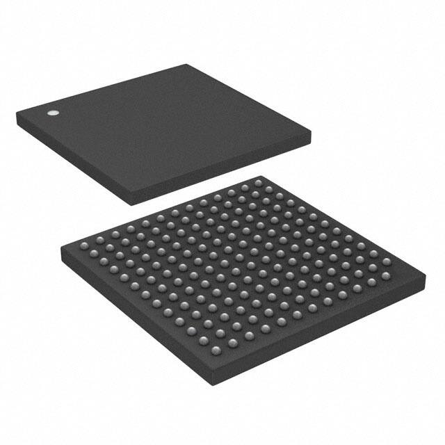
– 168-ball BGA (Pb-free)
• Revision
• 1066 MHz DDR operation (2133 Mb/s/ball data
rate)
• 76.8 Gb/s peak bandwidth (x36 at 1066 MHz clock
frequency)
• Organization
– 32 Meg x 18, and 16 Meg x 36 common I/O (CIO)
– 16 banks
• 1.2V center-terminated push/pull I/O
• 2.5V V EXT, 1.35V V DD, 1.2V V DDQ I/O
• Reduced cycle time (tRC (MIN) = 7.5 - 12ns)
• SDR addressing
• Programmable READ/WRITE latency (RL/WL) and
burst length
• Data mask for WRITE commands
• Differential input clocks (CK, CK#)
• Free-running differential input data clocks (DKx,
DKx#) and output data clocks (QKx, QKx#)
• On-die DLL generates CK edge-aligned data and
differential output data clock signals
• 64ms refresh (128K refresh per 64ms)
• 168-ball BGA package
• Ω or 60Ω matched impedance outputs
• Integrated on-die termination (ODT)
• Single or multibank writes
• Extended operating range (200–1066 MHz)
• READ training register
• Multiplexed and non-multiplexed addressing capabilities
• Mirror function
• Output driver and ODT calibration
• JTAG interface (IEEE 1149.1-2001)
09005aef84003617
576mb_rldram3.pdf - Rev. L 1/19 EN
Note:
1
Marking
-093F
-093E
-107E
-125F
-125E
-125
32M18
16M36
None
IT
RB
:A / :B
1. Not all options listed can be combined to
define an offered product. Use the part catalog search on www.micron.com for available offerings.
Micron Technology, Inc. reserves the right to change products or specifications without notice.
2016 Micron Technology, Inc. All rights reserved.
Products and specifications discussed herein are subject to change by Micron without notice.
�576Mb: x18, x36 RLDRAM 3
Features
Figure 1: 576Mb RLDRAM 3 Part Numbers
Example Part Number: MT44K16M36RB-093E:B
MT44K
:
Speed Temp
Configuration Package
Rev.
Revision
Rev.
Configuration
32 Meg x 18
32M18
16 Meg x 36
16M36
:A / :B
Temperature
Commercial
None
Industrial
IT
Package
168-ball BGA (Pb-free)
Speed Grade
RB
-093F tCK = 0.93ns (7.5ns t RC)
-093E tCK = 0.93ns (8ns t RC)
-107E tCK = 1.07ns (8ns tRC)
-125F tCK = 1.25ns (8ns tRC)
-125E tCK = 1.25ns (10ns tRC)
-125
tCK
= 1.25ns (12ns tRC)
BGA Part Marking Decoder
Due to space limitations, BGA-packaged components have an abbreviated part marking that is different from the
part number. Micron’s BGA Part Marking Decoder is available on Micron’s Web site at www.micron.com.
09005aef84003617
576mb_rldram3.pdf - Rev. L 1/19 EN
2
Micron Technology, Inc. reserves the right to change products or specifications without notice.
2016 Micron Technology, Inc. All rights reserved.
�576Mb: x18, x36 RLDRAM 3
Features
Contents
General Description ......................................................................................................................................... 9
General Notes .............................................................................................................................................. 9
State Diagram ................................................................................................................................................ 10
Functional Block Diagrams ............................................................................................................................. 11
Ball Assignments and Descriptions ................................................................................................................. 13
Package Dimensions ....................................................................................................................................... 17
Electrical Characteristics – IDD Specifications .................................................................................................. 18
Electrical Specifications – Absolute Ratings and I/O Capacitance ..................................................................... 25
Absolute Maximum Ratings ........................................................................................................................ 25
Input/Output Capacitance .......................................................................................................................... 25
AC and DC Operating Conditions .................................................................................................................... 26
AC Overshoot/Undershoot Specifications .................................................................................................... 28
Slew Rate Definitions for Single-Ended Input Signals ................................................................................... 31
Slew Rate Definitions for Differential Input Signals ...................................................................................... 33
ODT Characteristics ....................................................................................................................................... 34
ODT Resistors ............................................................................................................................................ 34
ODT Sensitivity .......................................................................................................................................... 36
Output Driver Impedance ............................................................................................................................... 36
Output Driver Sensitivity ............................................................................................................................ 37
Output Characteristics and Operating Conditions ............................................................................................ 39
Reference Output Load ............................................................................................................................... 42
Slew Rate Definitions for Single-Ended Output Signals ..................................................................................... 43
Slew Rate Definitions for Differential Output Signals ........................................................................................ 44
Speed Bin Tables ............................................................................................................................................ 45
AC Electrical Characteristics ........................................................................................................................... 47
Temperature and Thermal Impedance Characteristics ..................................................................................... 53
Command and Address Setup, Hold, and Derating ........................................................................................... 55
Data Setup, Hold, and Derating ....................................................................................................................... 62
Commands .................................................................................................................................................... 69
MODE REGISTER SET (MRS) Command ......................................................................................................... 70
Mode Register 0 (MR0) .................................................................................................................................... 71
tRC ............................................................................................................................................................. 72
Data Latency .............................................................................................................................................. 72
DLL Enable/Disable ................................................................................................................................... 72
Address Multiplexing .................................................................................................................................. 72
Mode Register 1 (MR1) .................................................................................................................................... 74
Output Drive Impedance ............................................................................................................................ 74
DQ On-Die Termination (ODT) ................................................................................................................... 74
DLL Reset ................................................................................................................................................... 74
ZQ Calibration ............................................................................................................................................ 75
ZQ Calibration Long ................................................................................................................................... 76
ZQ Calibration Short ................................................................................................................................... 76
AUTO REFRESH Protocol ............................................................................................................................ 77
Burst Length (BL) ....................................................................................................................................... 77
Mode Register 2 (MR2) .................................................................................................................................... 79
READ Training Register (RTR) ..................................................................................................................... 79
WRITE Protocol .......................................................................................................................................... 81
WRITE Command .......................................................................................................................................... 81
Multibank WRITE ....................................................................................................................................... 82
READ Command ............................................................................................................................................ 82
09005aef84003617
576mb_rldram3.pdf - Rev. L 1/19 EN
3
Micron Technology, Inc. reserves the right to change products or specifications without notice.
2016 Micron Technology, Inc. All rights reserved.
�576Mb: x18, x36 RLDRAM 3
Features
AUTO REFRESH Command ............................................................................................................................ 84
INITIALIZATION Operation ............................................................................................................................ 86
WRITE Operation ........................................................................................................................................... 88
READ Operation ............................................................................................................................................. 92
AUTO REFRESH Operation ............................................................................................................................. 95
RESET Operation ............................................................................................................................................ 98
Clock Stop ...................................................................................................................................................... 99
Mirror Function ............................................................................................................................................ 100
Multiplexed Address Mode ............................................................................................................................. 101
Data Latency in Multiplexed Address Mode ................................................................................................ 106
REFRESH Command in Multiplexed Address Mode .................................................................................... 106
IEEE 1149.1 Serial Boundary Scan (JTAG) ....................................................................................................... 110
Disabling the JTAG Feature ........................................................................................................................ 110
Test Access Port (TAP) ................................................................................................................................ 110
TAP Controller ........................................................................................................................................... 111
Performing a TAP RESET ............................................................................................................................ 113
TAP Registers ............................................................................................................................................ 113
TAP Instruction Set .................................................................................................................................... 114
09005aef84003617
576mb_rldram3.pdf - Rev. L 1/19 EN
4
Micron Technology, Inc. reserves the right to change products or specifications without notice.
2016 Micron Technology, Inc. All rights reserved.
�576Mb: x18, x36 RLDRAM 3
Features
List of Figures
Figure 1: 576Mb RLDRAM 3 Part Numbers ..................................................................................................... 2
Figure 2: Simplified State Diagram ................................................................................................................. 10
Figure 3: 32 Meg x 18 Functional Block Diagram ............................................................................................. 11
Figure 4: 16 Meg x 36 Functional Block Diagram ............................................................................................. 12
Figure 5: 168-Ball BGA ................................................................................................................................... 17
Figure 6: Single-Ended Input Signal ............................................................................................................... 27
Figure 7: Overshoot ....................................................................................................................................... 28
Figure 8: Undershoot .................................................................................................................................... 28
Figure 9: V IX for Differential Signals ................................................................................................................ 29
Figure 10: Single-Ended Requirements for Differential Signals ........................................................................ 30
Figure 11: Definition of Differential AC Swing and tDVAC ................................................................................ 30
Figure 12: Nominal Slew Rate Definition for Single-Ended Input Signals .......................................................... 32
Figure 13: Nominal Differential Input Slew Rate Definition for CK, CK#, DKx, and DKx# .................................. 33
Figure 14: ODT Levels and I-V Characteristics ................................................................................................ 34
Figure 15: Output Driver ................................................................................................................................ 37
Figure 16: DQ Output Signal .......................................................................................................................... 41
Figure 17: Differential Output Signal .............................................................................................................. 42
Figure 18: Reference Output Load for AC Timing and Output Slew Rate ........................................................... 42
Figure 19: Nominal Slew Rate Definition for Single-Ended Output Signals ....................................................... 43
Figure 20: Nominal Differential Output Slew Rate Definition for QKx, QKx# ..................................................... 44
Figure 21: Example Temperature Test Point Location ...................................................................................... 54
Figure 22: Nominal Slew Rate and tVAC for tIS (Command and Address - Clock) ............................................... 58
Figure 23: Nominal Slew Rate for tIH (Command and Address - Clock) ............................................................ 59
Figure 24: Tangent Line for tIS (Command and Address - Clock) ...................................................................... 60
Figure 25: Tangent Line for tIH (Command and Address - Clock) ..................................................................... 61
Figure 26: Nominal Slew Rate and tVAC for tDS (DQ - Strobe) .......................................................................... 65
Figure 27: Nominal Slew Rate for tDH (DQ - Strobe) ........................................................................................ 66
Figure 28: Tangent Line for tDS (DQ - Strobe) ................................................................................................. 67
Figure 29: Tangent Line for tDH (DQ - Strobe) ................................................................................................ 68
Figure 30: MRS Command Protocol ............................................................................................................... 70
Figure 31: MR0 Definition for Non-Multiplexed Address Mode ........................................................................ 71
Figure 32: MR1 Definition for Non-Multiplexed Address Mode ........................................................................ 74
Figure 33: ZQ Calibration Timing (ZQCL and ZQCS) ....................................................................................... 76
Figure 34: Read Burst Lengths ........................................................................................................................ 78
Figure 35: MR2 Definition for Non-Multiplexed Address Mode ........................................................................ 79
Figure 36: READ Training Function - Back-to-Back Readout ............................................................................ 80
Figure 37: WRITE Command ......................................................................................................................... 81
Figure 38: READ Command ........................................................................................................................... 83
Figure 39: Bank Address-Controlled AUTO REFRESH Command ..................................................................... 84
Figure 40: Multibank AUTO REFRESH Command ........................................................................................... 85
Figure 41: Power-Up/Initialization Sequence ................................................................................................. 87
Figure 42: WRITE Burst ................................................................................................................................. 88
Figure 43: Consecutive WRITE Bursts ............................................................................................................. 89
Figure 44: WRITE-to-READ ............................................................................................................................ 89
Figure 45: WRITE - DM Operation .................................................................................................................. 90
Figure 46: Consecutive Quad Bank WRITE Bursts ........................................................................................... 90
Figure 47: Interleaved READ and Quad Bank WRITE Bursts ............................................................................. 91
Figure 48: Basic READ Burst .......................................................................................................................... 92
Figure 49: Consecutive READ Bursts (BL = 2) .................................................................................................. 93
Figure 50: Consecutive READ Bursts (BL = 4) .................................................................................................. 93
09005aef84003617
576mb_rldram3.pdf - Rev. L 1/19 EN
5
Micron Technology, Inc. reserves the right to change products or specifications without notice.
2016 Micron Technology, Inc. All rights reserved.
�576Mb: x18, x36 RLDRAM 3
Features
Figure 51:
Figure 52:
Figure 53:
Figure 54:
Figure 55:
Figure 56:
Figure 57:
Figure 58:
Figure 59:
Figure 60:
Figure 61:
Figure 62:
Figure 63:
Figure 64:
Figure 65:
Figure 66:
Figure 67:
Figure 68:
Figure 69:
Figure 70:
Figure 71:
Figure 72:
READ-to-WRITE (BL = 2) ............................................................................................................... 94
Read Data Valid Window ................................................................................................................ 94
Bank Address-Controlled AUTO REFRESH Cycle ............................................................................. 95
Multibank AUTO REFRESH Cycle ................................................................................................... 95
READ Burst with ODT .................................................................................................................... 96
READ-NOP-READ with ODT .......................................................................................................... 97
RESET Sequence ........................................................................................................................... 98
Command Description in Multiplexed Address Mode .................................................................... 101
Power-Up/Initialization Sequence in Multiplexed Address Mode .................................................... 102
MR0 Definition for Multiplexed Address Mode ............................................................................... 103
MR1 Definition for Multiplexed Address Mode ............................................................................... 104
MR2 Definition for Multiplexed Address Mode ............................................................................... 105
Bank Address-Controlled AUTO REFRESH Operation with Multiplexed Addressing ......................... 106
Multibank AUTO REFRESH Operation with Multiplexed Addressing ............................................... 106
Consecutive WRITE Bursts with Multiplexed Addressing ................................................................ 107
WRITE-to-READ with Multiplexed Addressing ............................................................................... 108
Consecutive READ Bursts with Multiplexed Addressing .................................................................. 108
READ-to-WRITE with Multiplexed Addressing ............................................................................... 109
TAP Controller State Diagram ........................................................................................................ 112
TAP Controller Functional Block Diagram ..................................................................................... 112
JTAG Operation - Loading Instruction Code and Shifting Out Data ................................................. 115
TAP Timing .................................................................................................................................. 116
09005aef84003617
576mb_rldram3.pdf - Rev. L 1/19 EN
6
Micron Technology, Inc. reserves the right to change products or specifications without notice.
2016 Micron Technology, Inc. All rights reserved.
�576Mb: x18, x36 RLDRAM 3
Features
List of Tables
Table 1: 32 Meg x 18 Ball Assignments – 168-Ball BGA (Top View) .................................................................... 13
Table 2: 16 Meg x 36 Ball Assignments – 168-Ball BGA (Top View) .................................................................... 14
Table 3: Ball Descriptions .............................................................................................................................. 15
Table 4: IDD Operating Conditions and Maximum Limits (Die Rev :A) .............................................................. 18
Table 5: IDD Operating Conditions and Maximum Limits (Die Rev :B ) ............................................................. 22
Table 6: Absolute Maximum Ratings .............................................................................................................. 25
Table 7: Input/Output Capacitance ................................................................................................................ 25
Table 8: DC Electrical Characteristics and Operating Conditions ..................................................................... 26
Table 9: Input AC Logic Levels ........................................................................................................................ 26
Table 10: Control and Address Balls ................................................................................................................ 28
Table 11: Clock, Data, Strobe, and Mask Balls ................................................................................................. 28
Table 12: Differential Input Operating Conditions (CK, CK# and DKx, DKx#) ................................................... 29
Table 13: Allowed Time Before Ringback ( tDVAC) for CK, CK#, DKx, and DKx# ................................................. 31
Table 14: Single-Ended Input Slew Rate Definition .......................................................................................... 31
Table 15: Differential Input Slew Rate Definition ............................................................................................. 33
Table 16: ODT DC Electrical Characteristics ................................................................................................... 34
Table 17: RTT Effective Impedances ................................................................................................................ 35
Table 18: ODT Sensitivity Definition .............................................................................................................. 36
Table 19: ODT Temperature and Voltage Sensitivity ........................................................................................ 36
Table 20: Driver Pull-Up and Pull-Down Impedance Calculations ................................................................... 37
Table 21: Output Driver Sensitivity Definition ................................................................................................. 38
Table 22: Output Driver Voltage and Temperature Sensitivity .......................................................................... 38
Table 23: Single-Ended Output Driver Characteristics ..................................................................................... 39
Table 24: Differential Output Driver Characteristics ........................................................................................ 40
Table 25: Single-Ended Output Slew Rate Definition ....................................................................................... 43
Table 26: Differential Output Slew Rate Definition .......................................................................................... 44
Table 27: RL3 2133/1866 Speed Bins ............................................................................................................... 45
Table 28: RL3 1600 Speed Bins ....................................................................................................................... 46
Table 29: AC Electrical Characteristics ............................................................................................................ 47
Table 30: Temperature Limits ......................................................................................................................... 53
Table 31: Thermal Impedance ........................................................................................................................ 53
Table 32: Command and Address Setup and Hold Values Referenced at 1 V/ns – AC/DC-Based ........................ 55
Table 33: Derating Values for tIS/tIH – AC150/DC100-Based ............................................................................ 56
Table 34: Derating Values for tIS/tIH – AC120/DC100-Based ............................................................................ 57
Table 35: Minimum Required Time tVAC Above V IH(AC) (or Below V IL(AC)) for Valid Transition ............................ 57
Table 36: Data Setup and Hold Values at 1 V/ns (DKx, DKx# at 2V/ns) – AC/DC-Based ..................................... 62
Table 37: Derating Values for tDS/tDH – AC150/DC100-Based ......................................................................... 63
Table 38: Derating Values for tDS/tDH – AC120/DC100-Based ......................................................................... 64
Table 39: Minimum Required Time tVAC Above V IH(AC) (or Below V IL(AC)) for Valid Transition ............................ 64
Table 40: Command Descriptions .................................................................................................................. 69
Table 41: Command Table ............................................................................................................................. 69
Table 42: tRC_MRS Values .............................................................................................................................. 72
Table 43: Address Widths of Different Burst Lengths ....................................................................................... 77
Table 44: 32 Meg x 18 Ball Assignments with MF Ball Tied HIGH ..................................................................... 100
Table 45: Address Mapping in Multiplexed Address Mode .............................................................................. 105
Table 46: TAP Input AC Logic Levels .............................................................................................................. 116
Table 47: TAP AC Electrical Characteristics .................................................................................................... 116
Table 48: TAP DC Electrical Characteristics and Operating Conditions ............................................................ 117
Table 49: Identification Register Definitions .................................................................................................. 117
Table 50: Scan Register Sizes ......................................................................................................................... 118
09005aef84003617
576mb_rldram3.pdf - Rev. L 1/19 EN
7
Micron Technology, Inc. reserves the right to change products or specifications without notice.
2016 Micron Technology, Inc. All rights reserved.
�576Mb: x18, x36 RLDRAM 3
Features
Table 51: Instruction Codes .......................................................................................................................... 118
Table 52: Boundary Scan (Exit), Die Rev. A ..................................................................................................... 118
Table 53: Boundary Scan (Exit), Die Rev. B ..................................................................................................... 120
09005aef84003617
576mb_rldram3.pdf - Rev. L 1/19 EN
8
Micron Technology, Inc. reserves the right to change products or specifications without notice.
2016 Micron Technology, Inc. All rights reserved.
�576Mb: x18, x36 RLDRAM 3
General Description
General Description
The Micron RLDRAM 3 is a high-speed memory device designed for high-bandwidth
data storage—telecommunications, networking, cache applications, and so forth. The
chip’s 16-bank architecture is optimized for sustainable high-speed operation.
The DDR I/O interface transfers two data bits per clock cycle at the I/O balls. Output
data is referenced to the READ strobes.
Commands, addresses, and control signals are also registered at every positive edge of
the differential input clock, while input data is registered at both positive and negative
edges of the input data strobes.
Read and write accesses to the RL3 device are burst-oriented. The burst length (BL) is
programmable to 2, 4, or 8 by a setting in the mode register.
The device is supplied with 1.35V for the core and 1.2V for the output drivers. The 2.5V
supply is used for an internal supply.
Bank-scheduled refresh is supported with the row address generated internally.
The 168-ball BGA package is used to enable ultra-high-speed data transfer rates.
General Notes
• The functionality and the timing specifications discussed in this data sheet are for the
DLL enable mode of operation.
• Any functionality not specifically stated is considered undefined, illegal, and not supported, and can result in unknown operation.
• Nominal conditions are assumed for specifications not defined within the figures
shown in this data sheet.
• Throughout this data sheet, the terms "RLDRAM," "DRAM,” and "RLDRAM 3" are all
used interchangeably and refer to the RLDRAM 3 SDRAM device.
• References to DQ, DK, QK, DM, and QVLD are to be interpreted as each group collectively, unless specifically stated otherwise. This includes true and complement signals
of differential signals.
• Non-multiplexed operation is assumed if not specified as multiplexed.
• A x36 device supplies four QK/QK# sets, one per nine DQ. Using only two QK/QK#
sets is allowed, but QK0/QK0# and QK1/QK1# must be used. QK0/QK0# control
DQ[8:0] and DQ[26:18], and QK1/QK1# control DQ[17:9] and DQ[35:27]. The QK to
DQ timing parameter to be used is tQKQ02, tQKQ13. The unused QK/QK# pins should
be left floating.
09005aef84003617
576mb_rldram3.pdf - Rev. L 1/19 EN
9
Micron Technology, Inc. reserves the right to change products or specifications without notice.
2016 Micron Technology, Inc. All rights reserved.
�576Mb: x18, x36 RLDRAM 3
State Diagram
State Diagram
Figure 2: Simplified State Diagram
Initialization
sequence
NOP
READ
WRITE
RESET#
MRS
AREF
Automatic sequence
Command sequence
09005aef84003617
576mb_rldram3.pdf - Rev. L 1/19 EN
10
Micron Technology, Inc. reserves the right to change products or specifications without notice.
2016 Micron Technology, Inc. All rights reserved.
�09005aef84003617
576mb_rldram3.pdf - Rev. L 1/19 EN
Functional Block Diagrams
Figure 3: 32 Meg x 18 Functional Block Diagram
ZQ
ZQ CAL
ZQ CAL
RZQ
ZQCL, ZQCS
ODT control
CK
CK#
Command
decode
CS#
REF#
WE#
Control
logic
VDDQ/2
Bank 15
Bank 14
RTT
MF
RESET#
Mode register
Refresh
counter
24
ODT control
Bank 1
Bank 0
13
Rowaddress
MUX
13
13
Bank 0
rowaddress
latch
and
decoder
8192
DLL
ZQ CAL
18
11
18
144
SENSE
AMPLIFIERS
Sense amplifiers
READ n
logic
n
18
DQ
latch
4
144
Address
register
Bank
control
logic
4
VDDQ/2
I/O gating
DQM mask logic
16
2
RTT
16
ODT control
18
5
8
TMS
TDI
JTAG
Logic and
Boundary
Scan Register
71
Column
decoder
WRITE
FIFO
and
drivers
CLK
in
71
(0...3)
RCVRS
18
18
Input
logic
144
TCK
DQ[17:0]
1
32
Columnaddress
counter/
latch
QK0/QK0#,QK1/QK1#
4
DK0/DK0#, DK1/DK1#
VDDQ/2
RTT
21
ODT control
2
DM[1:0]
TDO
Notes:
1. Example for BL = 2; column address will be reduced with an increase in burst length.
2. 8 = (length of burst) x 2^ (number of column addresses to WRITE FIFO and READ logic).
576Mb: x18, x36 RLDRAM 3
Functional Block Diagrams
Micron Technology, Inc. reserves the right to change products or specifications without notice.
2016 Micron Technology, Inc. All rights reserved.
24
QVLD
READ
Drivers
QK/QK#
generator
8192
A[19:0]1
BA[3:0]
(0 ....17)
CK/CK#
Bank 0
memory
array
(8192 x 32 x 8 x 18)2
�09005aef84003617
576mb_rldram3.pdf - Rev. L 1/19 EN
Functional Block Diagrams
Figure 4: 16 Meg x 36 Functional Block Diagram
ZQ
ZQ CAL
ZQ CAL
RZQ
ZQCL, ZQCS
ODT control
CK
CK#
Command
decode
CS#
REF#
WE#
Control
logic
VDDQ/2
Bank 15
Bank 14
RTT
MF
RESET#
Refresh
counter
Mode register
23
ODT control
Bank 1
Bank 0
13
Rowaddress
MUX
13
13
Bank 0
rowaddress
latch
and
decoder
8192
36
12
36
144
READ n
logic
n
36
READ
Drivers
DQ
latch
4
16
ODT control
(0...3)
16
4
32
8
TCK
TMS
TDI
JTAG
Logic and
Boundary
Scan Register
61
Column
decoder
WRITE
FIFO
and
drivers
CLK
in
61
36
36
36
DK0/DK0#, DK1/DK1#
RCVRS
Input
logic
144
5
Columnaddress
counter/
latch
DQ[35:0]
RTT
11
I/O gating
DQM mask logic
VDDQ/2
RTT
11
ODT control
2
DM[1:0]
TDO
Notes:
1. Example for BL = 2; column address will be reduced with an increase in burst length.
2. 4 = (length of burst) x 2^ (number of column addresses to WRITE FIFO and READ logic).
576Mb: x18, x36 RLDRAM 3
Functional Block Diagrams
Micron Technology, Inc. reserves the right to change products or specifications without notice.
2016 Micron Technology, Inc. All rights reserved.
Bank
control
logic
QK0/QK0#, QK1/QK1#
QK2/QK2#, QK3/QK3#
VDDQ/2
144
Address
register
QVLD[1:0]
8
QK/QK#
generator
8192
23
DLL
ZQ CAL
SENSEamplifiers
AMPLIFIERS
Sense
A[18:0]1
BA[3:0]
(0 ....35)
CK/CK#
Bank 0
memory
array
(8192 x 32 x 4 x 36)2
�576Mb: x18, x36 RLDRAM 3
Ball Assignments and Descriptions
Ball Assignments and Descriptions
Table 1: 32 Meg x 18 Ball Assignments – 168-Ball BGA (Top View)
1
A
2
3
4
5
6
7
8
9
10
11
12
13
VSS
VDD
NF
VDDQ
NF
VREF
DQ7
VDDQ
DQ8
VDD
VSS
RESET#
B
VEXT
VSS
NF
VSSQ
NF
VDDQ
DM0
VDDQ
DQ5
VSSQ
DQ6
VSS
VEXT
C
VDD
NF
VDDQ
NF
VSSQ
NF
DK0#
DQ2
VSSQ
DQ3
VDDQ
DQ4
VDD
D
A11
VSSQ
NF
VDDQ
NF
VSSQ
DK0
VSSQ
QK0
VDDQ
DQ0
VSSQ
A13
E
VSS
A0
VSSQ
NF
VDDQ
NF
MF
QK0#
VDDQ
DQ1
VSSQ
CS#
VSS
1
F
A7
NF(CS1/A20)
VDD
A2
A1
WE#
ZQ
REF#
A3
A4
VDD
A5
A9
G
VSS
A15
A6
VSS
BA1
VSS
CK#
VSS
BA0
VSS
A8
A18
VSS (RFU)2
H
A19
VDD
A14
A16
VDD
BA3
CK
BA2
VDD
A17
A12
VDD
A10
J
VDDQ
NF
VSSQ
NF
VDDQ
NF
VSS
QK1#
VDDQ
DQ9
VSSQ
QVLD
VDDQ
K
NF
VSSQ
NF
VDDQ
NF
VSSQ
DK1
VSSQ
QK1
VDDQ
DQ10
VSSQ
DQ11
L
VDD
NF
VDDQ
NF
VSSQ
NF
DK1#
DQ12
VSSQ
DQ13
VDDQ
DQ14
VDD
M
VEXT
VSS
NF
VSSQ
NF
VDDQ
DM1
VDDQ
DQ15
VSSQ
DQ16
VSS
VEXT
N
VSS
TCK
VDD
TDO
VDDQ
NF
VREF
DQ17
VDDQ
TDI
VDD
TMS
VSS
Notes:
09005aef84003617
576mb_rldram3.pdf - Rev. L 1/19 EN
1. F2 is an NF ball for both the X18 & X36 576Mb devices, but is also the Location of CS1 to
support the 1Gb x18 DDP device. This same ball has been designated as the location of
A20 for the future 1Gb monolithic device. F2 is Internally connected so it can mirror the
A5 address signal when MF is asserted HIGH and has parasitic characteristics of an address pin.
2. G13 is a VSS ball for both X18 & X36 576Mb devices, but has been reserved for future
use (RFU) on the 1Gb monolithic devices and will have parasitic characteristics of an address.
3. NF balls for the x18 configuration are internally connected and have parasitic characteristics of an I/O. Balls may be connected to VSSQ.
4. MF is assumed to be tied LOW for this ball assignment.
13
Micron Technology, Inc. reserves the right to change products or specifications without notice.
2016 Micron Technology, Inc. All rights reserved.
�576Mb: x18, x36 RLDRAM 3
Ball Assignments and Descriptions
Table 2: 16 Meg x 36 Ball Assignments – 168-Ball BGA (Top View)
1
A
2
3
4
5
6
7
8
9
10
11
12
13
VSS
VDD
DQ26
VDDQ
DQ25
VREF
DQ7
VDDQ
DQ8
VDD
VSS
RESET#
B
VEXT
VSS
DQ24
VSSQ
DQ23
VDDQ
DM0
VDDQ
DQ5
VSSQ
DQ6
VSS
VEXT
C
VDD
DQ22
VDDQ
DQ21
VSSQ
DQ20
DK0#
DQ2
VSSQ
DQ3
VDDQ
DQ4
VDD
D
A11
VSSQ
DQ18
VDDQ
QK2
VSSQ
DK0
VSSQ
QK0
VDDQ
DQ0
VSSQ
A13
E
VSS
A0
VSSQ
DQ19
VDDQ
QK2#
MF
QK0#
VDDQ
DQ1
VSSQ
CS#
VSS
1
F
A7
NF(CS1/A20)
VDD
A2
A1
WE#
ZQ
REF#
A3
A4
VDD
A5
A9
G
VSS
A15
A6
VSS
BA1
VSS
CK#
VSS
BA0
VSS
A8
A18
VSS (RFU)2
H
NF(A19)3
VDD
A14
A16
VDD
BA3
CK
BA2
VDD
A17
A12
VDD
A10
J
VDDQ
QVLD1
VSSQ
DQ27
VDDQ
QK3#
VSS
QK1#
VDDQ
DQ9
VSSQ
QVLD0
VDDQ
K
DQ29
VSSQ
DQ28
VDDQ
QK3
VSSQ
DK1
VSSQ
QK1
VDDQ
DQ10
VSSQ
DQ11
L
VDD
DQ32
VDDQ
DQ31
VSSQ
DQ30
DK1#
DQ12
VSSQ
DQ13
VDDQ
DQ14
VDD
M
VEXT
VSS
DQ34
VSSQ
DQ33
VDDQ
DM1
VDDQ
DQ15
VSSQ
DQ16
VSS
VEXT
N
VSS
TCK
VDD
TDO
VDDQ
DQ35
VREF
DQ17
VDDQ
TDI
VDD
TMS
VSS
Notes:
09005aef84003617
576mb_rldram3.pdf - Rev. L 1/19 EN
1. F2 is an NF ball for both the X18 & X36 576Mb devices, but is also the Location of CS1 to
support the 1Gb x18 DDP device. This same ball has been designated as the location of
A20 for the future 1Gb monolithic device. F2 is Internally connected so it can mirror the
A5 address signal when MF is asserted HIGH and has parasitic characteristics of an address pin.
2. G13 is a VSS ball for both X18 & X36 576Mb devices, but has been reserved for future
use (RFU) on the 1Gb monolithic devices and will have parasitic characteristics of an address.
3. NF ball for x36 configuration is internally connected and has parasitic characteristics of
an address (A19 for x18 configuration). Ball may be connected to VSSQ.
4. MF is assumed to be tied LOW for this ball assignment.
14
Micron Technology, Inc. reserves the right to change products or specifications without notice.
2016 Micron Technology, Inc. All rights reserved.
�576Mb: x18, x36 RLDRAM 3
Ball Assignments and Descriptions
Table 3: Ball Descriptions
Symbol
Type
Description
A[19:0]
Input
Address inputs: A[19:0] define the row and column addresses for READ and WRITE operations.
During a MODE REGISTER SET, the address inputs define the register settings along with BA[3:0].
They are sampled at the rising edge of CK.
BA[3:0]
Input
Bank address inputs: Select the internal bank to which a command is being applied.
CK/CK#
Input
Input clock: CK and CK# are differential input clocks. Addresses and commands are latched on
the rising edge of CK.
CS#
Input
Chip select: CS# enables the command decoder when LOW and disables it when HIGH. When
the command decoder is disabled, new commands are ignored, but internal operations continue.
DQ[35:0]
I/O
Data input: The DQ signals form the 36-bit data bus. During READ commands, the data is referenced to both edges of QK. During WRITE commands, the data is sampled at both edges of DK.
DKx, DKx#
Input
Input data clock: DKx and DKx# are differential input data clocks. All input data is referenced
to both edges of DKx. For the x36 device, DQ[8:0] and DQ[26:18] are referenced to DK0 and
DK0#, and DQ[17:9] and DQ[35:27] are referenced to DK1 and DK1#. For the x18 device, DQ[8:0]
are referenced to DK0 and DK0#, and DQ[17:9] are referenced to DK1 and DK1#. DKx and DKx#
are free-running signals and must always be supplied to the device.
DM[1:0]
Input
Input data mask: DM is the input mask signal for WRITE data. Input data is masked when DM
is sampled HIGH. DM0 is used to mask the lower byte for the x18 device and DQ[8:0] and
DQ[26:18] for the x36 device. DM1 is used to mask the upper byte for the x18 device and
DQ[17:9] and DQ[35:27] for the x36 device. Tie DM[1:0] to VSS if not used.
TCK
Input
IEEE 1149.1 clock input: This ball must be tied to VSS if the JTAG function is not used.
TMS, TDI
Input
IEEE 1149.1 test inputs: These balls may be left as no connects if the JTAG function is not used.
WE#, REF#
Input
Command inputs: Sampled at the positive edge of CK, WE# and REF# (together with CS#) define the command to be executed.
RESET#
Input
Reset: RESET# is an active LOW CMOS input referenced to VSS. RESET# assertion and deassertion
are asynchronous. RESET# is a CMOS input defined with DC HIGH ≥ 0.8 x VDDQ and DC LOW ≤ 0.2
x VDDQ.
ZQ
Input
External impedance: This signal is used to tune the device’s output impedance and ODT. RZQ
needs to be 240Ω, where RZQ is a resistor from this signal to ground.
QKx, QKx#
Output
Output data clocks: QK and QK# are opposite-polarity output data clocks. They are free-running signals and during READ commands are edge-aligned with the DQs. For the x36 device,
QK0, QK0# align with DQ[8:0]; QK1, QK1# align with DQ[17:9]; QK2, QK2# align with DQ[26:18];
QK3, QK3# align with DQ[35:27]. For the x18 device, QK0, QK0# align with DQ[8:0]; QK1, QK1#
align with DQ[17:9].
QVLDx
Output
Data valid: The QVLD ball indicates that valid output data will be available on the subsequent
rising clock edge. There is a single QVLD ball for the x18 device and two, QVLD0 and QVLD1, for
the x36 device. QVLD0 aligns with DQ[17:0]; QVLD1 aligns with DQ[35:18].
MF
Input
Mirror function: The mirror function ball is a DC input used to create mirrored ballouts for simple dual-loaded clamshell mounting. If the ball is tied to VSS, the address and command balls are
in their true layout. If the ball is tied to VDDQ, they are in the complement location. MF must be
tied HIGH or LOW and cannot be left floating.
TDO
Output
IEEE 1149.1 test output: JTAG output. This ball may be left as no connect if the JTAG function
is not used.
09005aef84003617
576mb_rldram3.pdf - Rev. L 1/19 EN
15
Micron Technology, Inc. reserves the right to change products or specifications without notice.
2016 Micron Technology, Inc. All rights reserved.
�576Mb: x18, x36 RLDRAM 3
Ball Assignments and Descriptions
Table 3: Ball Descriptions (Continued)
Symbol
Type
VDD
Supply
Power supply: 1.35V nominal. See Table 8 (page 26) for range.
VDDQ
Supply
DQ power supply: 1.2V nominal. Isolated on the device for improved noise immunity. See Table 8 (page 26) for range.
VEXT
Supply
Power supply: 2.5V nominal. See Table 8 (page 26) for range.
VREF
Supply
Input reference voltage: VDDQ/2 nominal. Provides a reference voltage for the input buffers.
VSS
Supply
Ground.
VSSQ
Supply
DQ ground: Isolated on the device for improved noise immunity.
NC
–
No connect: These balls are not connected to the DRAM.
NF
–
No function: These balls are connected to the DRAM, but provide no functionality.
09005aef84003617
576mb_rldram3.pdf - Rev. L 1/19 EN
Description
16
Micron Technology, Inc. reserves the right to change products or specifications without notice.
2016 Micron Technology, Inc. All rights reserved.
�576Mb: x18, x36 RLDRAM 3
Package Dimensions
Package Dimensions
Figure 5: 168-Ball BGA
Seating plane
A
168X Ø0.55
Dimensions apply
to solder balls postreflow on Ø0.40 NSMD
ball pads.
0.12 A
Ball A1 ID
(covered by SR)
13 12
11 10
9
8
7
6
5
4
3
2
Ball A1 ID
1
A
B
C
D
13.5 ±0.1
E
F
G
12 CTR
H
J
K
L
M
1 TYP
N
1 TYP
1.1 ±0.1
12 CTR
0.3 MIN
13.5 ±0.1
Notes:
09005aef84003617
576mb_rldram3.pdf - Rev. L 1/19 EN
1. All dimensions are in millimeters.
2. Solder ball material: SAC302 (96.8% Sn, 3% Ag, 0.2% Cu).
17
Micron Technology, Inc. reserves the right to change products or specifications without notice.
2016 Micron Technology, Inc. All rights reserved.
�09005aef84003617
576mb_rldram3.pdf - Rev. L 1/19 EN
Electrical Characteristics – IDD Specifications
Table 4: IDD Operating Conditions and Maximum Limits (Die Rev :A)
Notes 1–6 apply to the entire table
Description
Condition
-125E
-125
tCK
= idle; All banks idle; No inputs toggling
ISB1 (VDD) x18
125
125
125
125
125
ISB1 (VDD) x36
125
125
125
125
125
ISB1 (VEXT)
30
30
30
30
30
Clock active
standby current
CS# = 1; No commands; Bank address incremented and half address/data change
once every four clock cycles
ISB2 (VDD) x18
870
815
725
725
725
ISB2 (VDD) x36
895
835
740
740
740
ISB2 (VEXT)
30
30
30
30
30
BL = 2; Sequential bank access; Bank transitions once every tRC; Half address transitions once every tRC; Read followed by
write sequence; Continuous data during
WRITE commands
IDD1 (VDD) x18
1175
1100
990
940
915
IDD1 (VDD) x36
1185
1110
1000
950
925
IDD1 (VEXT)
35
35
35
35
35
BL = 4; Sequential bank access; Bank transitions once every tRC; Half address transitions once every tRC; Read followed by
write sequence; Continuous data during
WRITE commands
IDD2 (VDD) x18
1205
1130
1020
970
945
IDD2 (VDD) x36
1215
1140
1030
980
950
IDD2 (VEXT)
35
35
35
35
35
BL = 8; Sequential bank access; Bank transitions once every tRC; Half address transitions once every tRC; Read followed by
write sequence; Continuous data during
WRITE commands
IDD3 (VDD) x18
1300
1200
1085
1030
1000
IDD3 (VDD) x36
NA
NA
N/A
NA
NA
IDD3 (VEXT)
35
35
35
35
35
Sixteen bank cyclic refresh using Bank Address Control AREF protocol; Command
bus remains in refresh for all sixteen
banks; DQs are High-Z and at VDDQ/2; Addresses are at VDDQ/2
IREF1 (VDD) x18
1550
1400
1230
1230
1230
IREF1 (VDD) x36
1570
1420
1245
1245
1245
IREF1 (VEXT)
80
75
70
70
70
Single bank refresh using Bank Address
Control AREF protocol; Sequential bank
access every 0.489μs; DQs are High-Z and
at VDDQ/2; Addresses are at VDDQ/2
IREF2 (VDD) x18
875
820
730
730
730
IREF2 (VDD) x36
900
840
745
745
745
IREF2 (VEXT)
30
30
30
30
30
Operational
current: BL2
Operational
current: BL4
18
Micron Technology, Inc. reserves the right to change products or specifications without notice.
2016 Micron Technology, Inc. All rights reserved.
Operational
current: BL8
Burst refresh
current
Distributed
refresh current
Symbol
-093E -107E
Units
Notes
mA
mA
mA
mA
mA
mA
mA
576Mb: x18, x36 RLDRAM 3
Electrical Characteristics – IDD Specifications
-125F
Standby
current
�09005aef84003617
576mb_rldram3.pdf - Rev. L 1/19 EN
Table 4: IDD Operating Conditions and Maximum Limits (Die Rev :A) (Continued)
Notes 1–6 apply to the entire table
Description
Condition
Multibank refresh Quad bank refresh using Multibank AREF
protocol; BL = 4; Cyclic bank access; Subcurrent:
ject to tSAW and tMMD specifications;
4 bank refresh
DQs are High-Z and at VDDQ/2; Bank addresses are at VDDQ/2
Symbol
-093E -107E
-125F
-125E
-125
IMBREF4 (VDD) x18
2130
2030
1885
1885
1645
IMBREF4 (VDD) x36
2155
2050
1900
1900
1660
IMBREF4 (VEXT)
130
115
105
105
105
IDD2W (VDD) x18
2110
1910
1665
1665
1665
IDD2W (VDD) x36
2290
2070
1805
1805
1805
IDD2W (VEXT)
80
75
70
70
70
BL = 2; Cyclic bank access; Half of address
bits change every clock cycle; Continuous
data; Measurement is taken during continuous WRITE
Operating burst
write current :
BL4
BL = 4; Cyclic bank access; Half of address
bits change every two clock cycles; Continuous data; Measurement is taken during
continuous WRITE
IDD4W (VDD) x18
1730
1590
1395
1395
1395
IDD4W (VDD) x36
1815
1665
1460
1460
1460
IDD4W (VEXT)
55
55
50
50
50
Operating burst
BL = 8; Cyclic bank access; Half of address
write current :BL8 bits change every four clock cycles; Continuous data; Measurement is taken during
continuous WRITE
IDD8W (VDD) x18
1475
1335
1190
1190
1190
IDD8W (VDD) x36
NA
NA
NA
NA
NA
IDD8W (VEXT)
45
40
40
40
40
Micron Technology, Inc. reserves the right to change products or specifications without notice.
2016 Micron Technology, Inc. All rights reserved.
Multibank write
current:
Dual bank write
BL = 4; Cyclic bank access using Dual Bank
WRITE; Half of address bits change every
two clock cycles; Continuous data; Measurement is taken during continuous
WRITE
IDBWR (VDD) x18
2305
2170
1885
1885
1885
IDBWR (VDD) x36
2400
2250
1960
1960
1960
IDBWR (VEXT)
80
75
70
70
70
Multibank write
current:
Quad bank write
BL = 4; Cyclic bank access using Quad Bank
WRITE; Half of address bits change every
two clock cycles; Continuous data; Measurement is taken during continuous
WRITE; Subject to tSAW specification
IQBWR (VDD) x18
2965
2890
2525
2525
2525
IQBWR (VDD) x36
3195
3000
2615
2615
2615
IQBWR (VEXT)
130
115
100
100
100
Operating burst
read current
example
BL = 2; Cyclic bank access; Half of address
bits change every clock cycle; Continuous
data; Measurement is taken during continuous READ
IDD2R (VDD) x18
2250
2045
1785
1785
1785
IDD2R (VDD) x36
2395
2180
1895
1895
1895
IDD2R (VEXT)
80
75
70
70
70
Operating burst
read current
example
BL = 4; Cyclic bank access; Half of address
bits change every two clock cycles; Continuous data; Measurement is taken during
continuous READ
IDD4R (VDD) x18
1740
1595
1400
1400
1400
IDD4R (VDD) x36
1835
1685
1475
1475
1475
IDD4R (VEXT)
55
55
50
50
50
Notes
mA
mA
mA
mA
mA
mA
mA
mA
576Mb: x18, x36 RLDRAM 3
Electrical Characteristics – IDD Specifications
19
Operating burst
write current :
BL2
Units
�09005aef84003617
576mb_rldram3.pdf - Rev. L 1/19 EN
Table 4: IDD Operating Conditions and Maximum Limits (Die Rev :A) (Continued)
Notes 1–6 apply to the entire table
Description
Condition
Operating burst
read current
example
BL = 8; Cyclic bank access; Half of address
bits change every four clock cycles; Continuous data; Measurement is taken during
continuous READ
Symbol
-093E -107E
-125F
-125E
-125
IDD8R (VDD) x18
1450
1315
1175
1175
1175
IDD8R (VDD) x36
NA
NA
NA
NA
NA
IDD8R (VEXT)
45
40
40
40
40
Units
Notes
mA
Micron Technology, Inc. reserves the right to change products or specifications without notice.
2016 Micron Technology, Inc. All rights reserved.
576Mb: x18, x36 RLDRAM 3
Electrical Characteristics – IDD Specifications
20
�576Mb: x18, x36 RLDRAM 3
Electrical Characteristics – IDD Specifications
Notes:
1. IDD specifications are tested after the device is properly initialized. 0°C ≤ TC ≤ +95°C;
+1.28V ≤ VDD ≤ +1.42V,+1.14V ≤ VDDQ ≤ +1.26V,+2.38V ≤ VEXT ≤ +2.63V,VREF = VDDQ/2.
2. IDD measurements use tCK (MIN), tRC (MIN), and minimum data latency (RL and WL).
3. Input slew rate is 1V/ns for single ended signals and 2V/ns for differential signals.
4. Definitions for IDD conditions:
• LOW is defined as VIN ≤ VIL(AC)MAX.
• HIGH is defined as VIN ≥ VIH(AC)MIN.
• Continuous data is defined as half the DQ signals changing between HIGH and LOW
every half clock cycle (twice per clock).
• Continuous address is defined as half the address signals changing between HIGH and
LOW every clock cycle (once per clock).
• Sequential bank access is defined as the bank address incrementing by one every tRC.
• Cyclic bank access is defined as the bank address incrementing by one for each command access. For BL = 2 this is every clock, for BL = 4 this is every other clock, and for
BL = 8 this is every fourth clock.
5. CS# is HIGH unless a READ, WRITE, AREF, or MRS command is registered. CS# never transitions more than once per clock cycle.
6. IDD parameters are specified with ODT disabled.
09005aef84003617
576mb_rldram3.pdf - Rev. L 1/19 EN
21
Micron Technology, Inc. reserves the right to change products or specifications without notice.
2016 Micron Technology, Inc. All rights reserved.
�09005aef84003617
576mb_rldram3.pdf - Rev. L 1/19 EN
Electrical Characteristics – IDD Specifications
Table 5: IDD Operating Conditions and Maximum Limits (Die Rev :B )
Notes 1–6 apply to the entire table
Description
Condition
Symbol
-093F
-093E
-107E
ISB1 (VDD) x18
225
225
225
ISB1 (VDD) x36
225
225
225
tCK
ISB1 (VEXT)
55
55
55
Clock active standby
current
CS# = 1; No commands; Bank address incremented
and half address/data change once every four clock
cycles
ISB2 (VDD) x18
605
605
570
ISB2 (VDD) x36
625
625
585
ISB2 (VEXT)
55
55
55
BL = 2; Sequential bank access; Bank transitions once
every tRC; Half address transitions once every tRC;
Read followed by write sequence; Continuous data
during WRITE commands
IDD1 (VDD) x18
1105
1040
975
IDD1 (VDD) x36
1115
1050
985
IDD1 (VEXT)
60
60
60
BL = 4; Sequential bank access; Bank transitions once
every tRC; Half address transitions once every tRC;
Read followed by write sequence; Continuous data
during WRITE commands
IDD2 (VDD) x18
1200
1130
1060
IDD2 (VDD) x36
1210
1140
1070
IDD2 (VEXT)
60
60
60
BL = 8; Sequential bank access; Bank transitions once
every tRC; Half address transitions once every tRC;
Read followed by write sequence; Continuous data
during WRITE commands
IDD3 (VDD) x18
1160
1095
1015
IDD3 (VDD) x36
NA
NA
NA
IDD3 (VEXT)
60
60
60
Sixteen bank cyclic refresh using Bank Address Control AREF protocol; Command bus remains in refresh
for all sixteen banks; DQs are High-Z and at VDDQ/2;
Addresses are at VDDQ/2
IREF1 (VDD) x18
1135
1135
1025
IREF1 (VDD) x36
1150
1150
1040
IREF1 (VEXT)
115
115
110
Distributed
refresh current
Single bank refresh using Bank Address Control AREF
protocol; Sequential bank access every 0.489μs; DQs
are High-Z and at VDDQ/2; Addresses are at VDDQ/2
IREF2 (VDD) x18
580
580
540
IREF2 (VDD) x36
595
595
555
IREF2 (VEXT)
55
55
55
Multibank refresh current:
4 bank refresh
Quad bank refresh using Multibank AREF protocol;
BL = 4; Cyclic bank access; Subject to tSAW and tMMD
specifications; DQs are High-Z and at VDDQ/2; Bank
addresses are at VDDQ/2
IMBREF4 (VDD) x18
1490
1490
1420
IMBREF4 (VDD) x36
1510
1510
1435
IMBREF4 (VEXT)
185
185
165
Operating burst write
current : BL2
BL = 2; Cyclic bank access; Half of address bits change
every clock cycle; Continuous data; Measurement is
taken during continuous WRITE
IDD2W (VDD) x18
1655
1655
1500
IDD2W (VDD) x36
1810
1810
1635
IDD2W (VEXT)
80
80
75
Operational
current: BL2
Operational
current: BL4
22
Operational
current: BL8
Micron Technology, Inc. reserves the right to change products or specifications without notice.
2016 Micron Technology, Inc. All rights reserved.
Burst refresh
current
= idle; All banks idle; No inputs toggling
Units
mA
mA
mA
mA
mA
mA
mA
mA
mA
576Mb: x18, x36 RLDRAM 3
Electrical Characteristics – IDD Specifications
Standby
current
�09005aef84003617
576mb_rldram3.pdf - Rev. L 1/19 EN
Table 5: IDD Operating Conditions and Maximum Limits (Die Rev :B ) (Continued)
Notes 1–6 apply to the entire table
Description
Condition
Symbol
-093F
-093E
-107E
1515
1515
1395
1595
1595
1465
IDD4W (VEXT)
75
75
70
BL = 8; Cyclic bank access; Half of address bits change
every four clock cycles; Continuous data; Measurement is taken during continuous WRITE
IDD8W (VDD) x18
1140
1140
1040
IDD8W (VDD) x36
NA
NA
NA
IDD8W (VEXT)
70
70
65
Multibank write current:
Dual bank write
BL = 4; Cyclic bank access using Dual Bank WRITE;
Half of address bits change every two clock cycles;
Continuous data; Measurement is taken during continuous WRITE
IDBWR (VDD) x18
2005
2005
1890
IDBWR (VDD) x36
2090
2090
1960
IDBWR (VEXT)
115
115
110
Multibank write current:
Quad bank write
BL = 4; Cyclic bank access using Quad Bank WRITE;
Half of address bits change every two clock cycles;
Continuous data; Measurement is taken during continuous WRITE; Subject to tSAW specification
IQBWR (VDD) x18
2620
2620
2565
IQBWR (VDD) x36
2840
2840
2665
IQBWR (VEXT)
200
200
175
Operating burst read
current
example
BL = 2; Cyclic bank access; Half of address bits change
every clock cycle; Continuous data; Measurement is
taken during continuous READ
IDD2R (VDD) x18
1715
1715
1560
IDD2R (VDD) x36
1835
1835
1670
IDD2R (VEXT)
80
80
75
Operating burst read
current
example
BL = 4; Cyclic bank access; Half of address bits change
every two clock cycles; Continuous data; Measurement is taken during continuous READ
IDD4R (VDD) x18
1510
1510
1380
IDD4R (VDD) x36
1595
1595
1465
IDD4R (VEXT)
75
75
70
Operating burst read
current
example
BL = 8; Cyclic bank access; Half of address bits change
every four clock cycles; Continuous data; Measurement is taken during continuous READ
IDD8R (VDD) x18
1135
1135
1040
IDD8R (VDD) x36
NA
NA
NA
IDD8R (VEXT)
70
70
65
Operating burst write
current :BL8
BL = 4; Cyclic bank access; Half of address bits change
every two clock cycles; Continuous data; Measurement is taken during continuous WRITE
mA
mA
mA
mA
23
mA
Micron Technology, Inc. reserves the right to change products or specifications without notice.
2016 Micron Technology, Inc. All rights reserved.
mA
mA
576Mb: x18, x36 RLDRAM 3
Electrical Characteristics – IDD Specifications
IDD4W (VDD) x18
IDD4W (VDD) x36
Operating burst write
current : BL4
Units
�576Mb: x18, x36 RLDRAM 3
Electrical Characteristics – IDD Specifications
Notes:
1. IDD specifications are tested after the device is properly initialized. 0°C ≤ TC ≤ +95°C;
+1.28V ≤ VDD ≤ +1.42V, +1.14V ≤ VDDQ ≤ +1.26V, +2.38V ≤ VEXT ≤ +2.63V, VREF = VDDQ/2.
2. IDD mesurements use tCK (MIN), tRC (MIN), and minimum data latency (RL and WL).
3. Input slew rate is 1 V/ns for single ended signals and 2 V/ns for differential signals.
4. Definitions for IDD conditions:
• LOW is defined as VIN ≤ VIL(AC)MAX.
• HIGH is defined as VIN ≥ VIH(AC)MIN.
• Continuous data is defined as half the DQ signals changing between HIGH and LOW
every half clock cycle (twice per clock).
• Continuous address is defined as half the address signals changing between HIGH and
LOW every clock cycle (once per clock).
• Sequential bank access is defined as the bank address incrementing by one every tRC.
• Cyclic bank access is defined as the bank address incrementing by one for each command access. For BL = 2 this is every clock, for BL = 4 this is every other clock, and for
BL = 8 this is every fourth clock.
5. CS# is HIGH unless a READ, WRITE, AREF, or MRS command is registered. CS# never transitions more than once per clock cycle.
6. IDD parameters are specified with ODT disabled.
09005aef84003617
576mb_rldram3.pdf - Rev. L 1/19 EN
24
Micron Technology, Inc. reserves the right to change products or specifications without notice.
2016 Micron Technology, Inc. All rights reserved.
�576Mb: x18, x36 RLDRAM 3
Electrical Specifications – Absolute Ratings and I/O Capacitance
Electrical Specifications – Absolute Ratings and I/O Capacitance
Absolute Maximum Ratings
Stresses greater than those listed may cause permanent damage to the device. This is a
stress rating only, and functional operation of the device at these or any other conditions outside those indicated in the operational sections of this specification is not implied. Exposure to absolute maximum rating conditions for extended periods may adversely affect reliability.
Table 6: Absolute Maximum Ratings
Symbol
Parameter
Min
Max
Units
VDD
VDD supply voltage relative to VSS
–0.4
1.975
V
VDDQ
Voltage on VDDQ supply relative to VSS
–0.4
1.66
V
Voltage on any ball relative to VSS
–0.4
1.66
V
Voltage on VEXT supply relative to VSS
–0.4
2.8
V
VIN,VOUT
VEXT
Input/Output Capacitance
Table 7: Input/Output Capacitance
Notes 1 and 2 apply to entire table
RL3-2133
Capacitance Parameters
Symbol
Min
CK/CK#
CCK
ΔC: CK to CK#
CDCK
Single-ended I/O: DQ, DM
Input strobe: DK/DK#
RL3-1866
Max
Min
1.3
2.1
0
0.15
CIO
1.9
CIO
1.9
RL3-1600
Max
Min
Max
Units
1.3
2.1
1.3
2.2
pF
0
0.15
0
0.15
pF
2.9
1.9
3.0
2.0
3.1
pF
2.9
1.9
3.0
2.0
3.1
pF
Notes
3
CIO
1.9
2.9
1.9
3.0
2.0
3.1
pF
ΔC: DK to DK#
CDDK
0
0.15
0
0.15
0
0.15
pF
ΔC: QK to QK#
CDQK
0
0.15
0
0.15
0
0.15
pF
ΔC: DQ to QK or DQ to DK
CDIO
–0.5
0.3
–0.5
0.3
–0.5
0.3
pF
4
Output strobe: QK/QK#, QVLD
Inputs (CMD, ADDR)
ΔC: CMD_ADDR to CK
JTAG balls
RESET#, MF balls
Notes:
09005aef84003617
576mb_rldram3.pdf - Rev. L 1/19 EN
CI
1.25
2.25
1.25
2.25
1.25
2.25
pF
5
CDI_CMD_ADDR
–0.5
0.3
–0.5
0.3
–0.4
0.4
pF
6
CJTAG
1.5
4.5
1.5
4.5
1.5
4.5
pF
7
CI
–
3.0
–
3.0
–
3.0
pF
1. +1.28V ≤ VDD ≤ +1.42V, +1.14V ≤ VDDQ ≤ 1.26V, +2.38V ≤ VEXT ≤ +2.63V, VREF = VSS, f = 100
MHz, TC = 25°C, VOUT(DC) = 0.5 × VDDQ, VOUT (peak-to-peak) = 0.1V.
2. Capacitance is not tested on ZQ ball.
3. DM input is grouped with the I/O balls, because they are matched in loading.
4. CDIO = CIO(DQ) - 0.5 × (CIO [QK] + CIO [QK#]).
5. Includes CS#, REF#, WE#, A[19:0], and BA[3:0].
6. CDI_CMD_ADDR = CI (CMD_ADDR) - 0.5 × (CCK [CK] + CCK [CK#]).
7. JTAG balls are tested at 50 MHz.
25
Micron Technology, Inc. reserves the right to change products or specifications without notice.
2016 Micron Technology, Inc. All rights reserved.
�576Mb: x18, x36 RLDRAM 3
AC and DC Operating Conditions
AC and DC Operating Conditions
Table 8: DC Electrical Characteristics and Operating Conditions
Note 1 applies to the entire table; Unless otherwise noted: 0°C ≤ TC ≤ +95°C; +1.28V ≤ VDD ≤ +1.42V
Description
Symbol
Min
Max
Units
Supply voltage
VEXT
2.38
2.63
V
Supply voltage
VDD
1.28
1.42
V
Isolated output buffer supply
VDDQ
1.14
1.26
V
Reference voltage
VREF
0.49 × VDDQ
0.51 × VDDQ
V
Input HIGH (logic 1) voltage
VIH(DC)
VREF + 0.10
VDDQ
V
Input LOW (logic 0) voltage
VIL(DC)
VSS
VREF - 0.10
V
Input leakage current: Any input 0V ≤ VIN ≤ VDD, VREF ball
0V ≤ VIN ≤ 1.1V (All other balls not under test = 0V)
ILI
–2
2
μA
Reference voltage current (All other balls not under test =
0V)
IREF
–5
5
μA
Notes:
Notes
2, 3
1. All voltages referenced to VSS (GND).
2. The nominal value of VREF is expected to be 0.5 × VDDQ of the transmitting device. VREF is
expected to track variations in VDDQ.
3. Peak-to-peak noise (non-common mode) on VREF may not exceed ±2% of the DC value.
DC values are determined to be less than 20 MHz. Peak-to-peak AC noise on VREF should
not exceed ±2% of VREF(DC). Thus, from VDDQ/2, VREF is allowed ±2% VDDQ/2 for DC error
and an additional ±2% VDDQ/2 for AC noise. The measurement is to be taken at the
nearest VREF bypass capacitor.
Table 9: Input AC Logic Levels
Notes 1-3 apply to entire table; Unless otherwise noted: 0°C ≤ TC ≤ +95°C; +1.28V ≤ VDD ≤ +1.42V
Description
Symbol
Min
Max
Units
Input HIGH (logic 1) voltage
VIH(AC150)
VREF + 0.15
–
V
Input HIGH (logic 1) voltage
VIH(AC120)
VREF + 0.12
–
V
Input LOW (logic 0) voltage
VIL(AC120)
–
VREF - 0.12
V
Input LOW (logic 0) voltage
VIL(AC150)
–
VREF - 0.15
V
Notes:
09005aef84003617
576mb_rldram3.pdf - Rev. L 1/19 EN
1. All voltages referenced to VSS (GND).
2. The receiver will effectively switch as a result of the signal crossing the AC input level,
and will remain in that state as long as the signal does not ring back above/below the
DC input LOW/HIGH level.
3. Single-ended input slew rate = 1 V/ns; maximum input voltage swing under test is
900mV (peak-to-peak).
26
Micron Technology, Inc. reserves the right to change products or specifications without notice.
2016 Micron Technology, Inc. All rights reserved.
�576Mb: x18, x36 RLDRAM 3
AC and DC Operating Conditions
Figure 6: Single-Ended Input Signal
VIL and VIH levels with ringback
1.60V
VDDQ + 0.4V narrow
pulse width
1.20V
VDDQ
Minimum VIL and VIH levels
0.750V
0.70V
VIH(AC)
VIH(DC)
0.624V
0.612V
0.60V
0.588V
0.576V
0.50V
0.45V
0.750V
VIH(AC)
0.70V
VIH(DC)
0.624V
0.612V
0.60V
0.588V
0.576V
VIL(DC)
VIL(AC)
VREF + AC noise
VREF + DC error
VREF - DC error
VREF - AC noise
0.50V
VIL(DC)
0.450V
VIL(AC)
VSS
0.0V
VSS - 0.4V narrow
pulse width
–0.40V
09005aef84003617
576mb_rldram3.pdf - Rev. L 1/19 EN
27
Micron Technology, Inc. reserves the right to change products or specifications without notice.
2016 Micron Technology, Inc. All rights reserved.
�576Mb: x18, x36 RLDRAM 3
AC and DC Operating Conditions
AC Overshoot/Undershoot Specifications
Table 10: Control and Address Balls
Parameter
RL3-2133
RL3-1866
RL3-1600
Maximum peak amplitude allowed for overshoot area
0.4V
0.4V
0.4V
Maximum peak amplitude allowed for undershoot area
0.4V
0.4V
0.4V
Maximum overshoot area above VDDQ
0.25 Vns
0.28 Vns
0.33 Vns
Maximum undershoot area below VSS/VSSQ
0.25 Vns
0.28 Vns
0.33 Vns
RL3-2133
RL3-1866
RL3-1600
Maximum peak amplitude allowed for overshoot area
0.4V
0.4V
0.4V
Maximum peak amplitude allowed for undershoot area
0.4V
0.4V
0.4V
Maximum overshoot area above VDDQ
0.10 Vns
0.11 Vns
0.13 Vns
Maximum undershoot area below VSS/VSSQ
0.10 Vns
0.11 Vns
0.13 Vns
Table 11: Clock, Data, Strobe, and Mask Balls
Parameter
Figure 7: Overshoot
Maximum amplitude
Overshoot area
Volts (V)
VDDQ
Time (ns)
Figure 8: Undershoot
VSS/VSSQ
Volts (V)
Undershoot area
Maximum amplitude
Time (ns)
09005aef84003617
576mb_rldram3.pdf - Rev. L 1/19 EN
28
Micron Technology, Inc. reserves the right to change products or specifications without notice.
2016 Micron Technology, Inc. All rights reserved.
�576Mb: x18, x36 RLDRAM 3
AC and DC Operating Conditions
Table 12: Differential Input Operating Conditions (CK, CK# and DKx, DKx#)
Notes 1 and 2 apply to entire table
Parameter/Condition
Symbol
Min
Differential input voltage logic HIGH – slew
VIH,diff_slew
+200
n/a
mV
3
Differential input voltage logic LOW – slew
VIL,diff_slew
n/a
-200
mV
3
Differential input voltage logic HIGH
VIH,diff(AC)
2 × (VIH(AC) - VREF)
VDDQ
mV
4
Differential input voltage logic LOW
VIL,diff(AC)
VSSQ
2 × (VIL(AC) - VREF )
mV
5
Differential input crossing voltage relative to VDD/2
Max
Units
Notes
VIX
VREF(DC) - 150
VREF(DC) + 150
mV
6
Single-ended HIGH level
VSEH
VIH(AC)
VDDQ
mV
4
Single-ended LOW level
VSEL
VSSQ
VIL(AC)
mV
5
Notes:
1.
2.
3.
4.
CK/CK# and DKx/DKx# are referenced to VDDQ and VSSQ.
Differential input slew rate = 2 V/ns.
Defines slew rate reference points, relative to input crossing voltages.
Maximum limit is relative to single-ended signals; overshoot specifications are applicable.
5. Minimum limit is relative to single-ended signals; undershoot specifications are applicable.
6. The typical value of VIX is expected to be about 0.5 × VDDQ of the transmitting device
and VIX is expected to track variations in VDDQ. VIX indicates the voltage at which differential input signals must cross.
Figure 9: VIX for Differential Signals
VDDQ
VDDQ
CK#, DKx#
CK#, DKx#
X
VIX
VIX
VDDQ/2
X
X
VDDQ/2
VIX
X
CK, DKx
CK, DKx
VSSQ
09005aef84003617
576mb_rldram3.pdf - Rev. L 1/19 EN
VIX
VSSQ
29
Micron Technology, Inc. reserves the right to change products or specifications without notice.
2016 Micron Technology, Inc. All rights reserved.
�576Mb: x18, x36 RLDRAM 3
AC and DC Operating Conditions
Figure 10: Single-Ended Requirements for Differential Signals
VDDQ
VSEH,min
VDDQ/2
VSEH
CK or DKx
VSEL,max
VSEL
VSS
Figure 11: Definition of Differential AC Swing and tDVAC
tDVAC
VIH,diff(AC)min
VIH,diff_slew,min
CK - CK#
DKx - DKx#
0.0
VIL,diff_slew,max
VIL,diff(AC)max
half cycle
09005aef84003617
576mb_rldram3.pdf - Rev. L 1/19 EN
30
tDVAC
Micron Technology, Inc. reserves the right to change products or specifications without notice.
2016 Micron Technology, Inc. All rights reserved.
�576Mb: x18, x36 RLDRAM 3
AC and DC Operating Conditions
Table 13: Allowed Time Before Ringback (tDVAC) for CK, CK#, DKx, and DKx#
Slew Rate (V/ns)
MIN tDVAC (ps) at |VIH/VIL,diff(AC)|
>4.0
175
4.0
170
3.0
167
2.0
163
1.9
162
1.6
161
1.4
159
1.2
155
1.0
150
2.0
175
2.0
170
1.5
167
1.0
163
0.9
162
0.8
161
0.7
159
0.6
155
0.5
150
2.0
175
2.0
170
1.5
167
1.0
163
0.9
162
0.8
161
0.7
159
0.6
155
0.5
150